

sergey23
-
Постов
15 -
Зарегистрирован
-
Посещение
Информация о sergey23
-
Звание
Участник
")
-
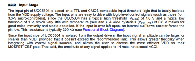
There are two components 74ABT04D Hex inverter and UCC5304DWVR gate driver. 74ABT04D Hex inverter is the signal genrator UCC5304DWVR is the reciever of the delayed signal. from section 8.3.2 of the data sheet shown below i see that the input load impedance is 200K which could be considered as open circuit. My LC ladder delay line caracteristic impedance Z=sqrt(L/C) neheds to match the load so i wont get ringing . but i dont want to do my LC ladder z0=200kOhm. I was told that a solution could besomething called series termination. i google it and so that its connecting a transmission line in series. 1.Is there a way to do series termination without transmission lines? 2.How exactly series termination will match my Z0 to the 200KOhm load? 3.Is it like a quarter wave transformer? Thanks. Thanks. https://www.mouser.co.il/datasheet/2/916/74ABT04-1541721.pdf https://www.ti.com/lit/ds/symlink/ucc5304.pdf?ts=1715329802200&ref_url=https%3A%2F%2Fwww.mouser.co.il%2F
-
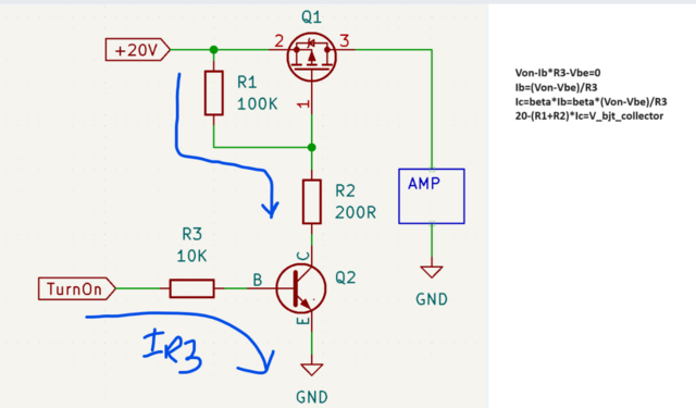
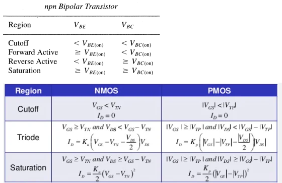
Just for the sake of knowledge i want to solve mathematickly the circuit i posted. I am trying to solve the equations for PMOS current threw the drain. A drawing of the currents on diagram shown in the attached photo. Von suppose its 5V for mathematical purposes how do i know the voltage potential at the collector of the bjt? so i could find the voltage at the gate of the PMOS afterwards Thanks. Von-Ib*R3-Vbe=0 Ib=(Von-Vbe)/R3 Ic=beta*Ib=beta*(Von-Vbe)/R3 20-(R1+R2)*Ic=V_bjt_collector Also i know that R1 is a sort of discharge for mosfet gate capacitor
-
general strategy will also be good. UPdate: The circuit is like this:
-
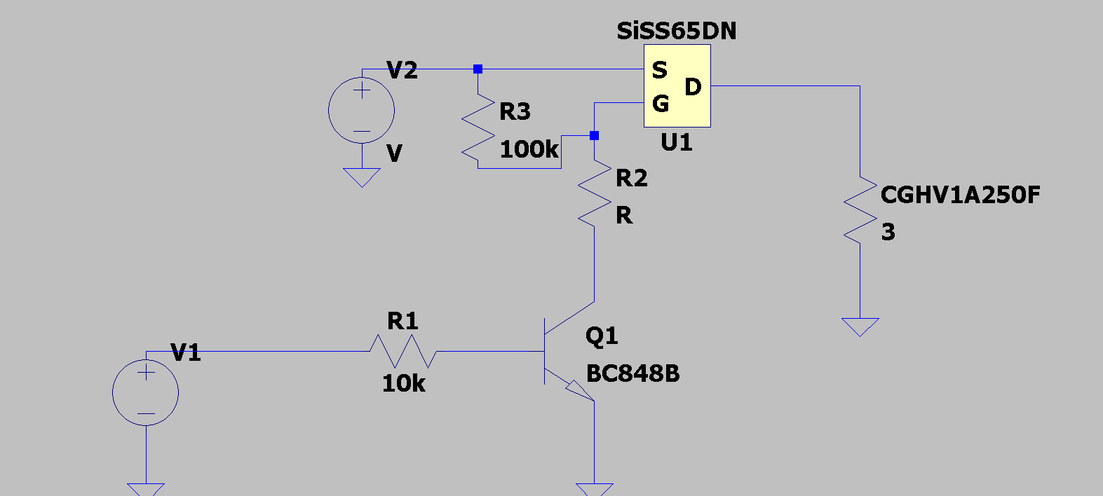
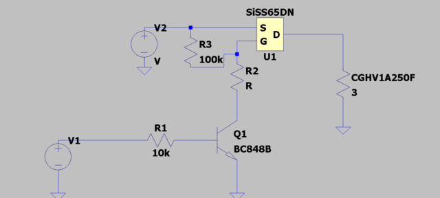
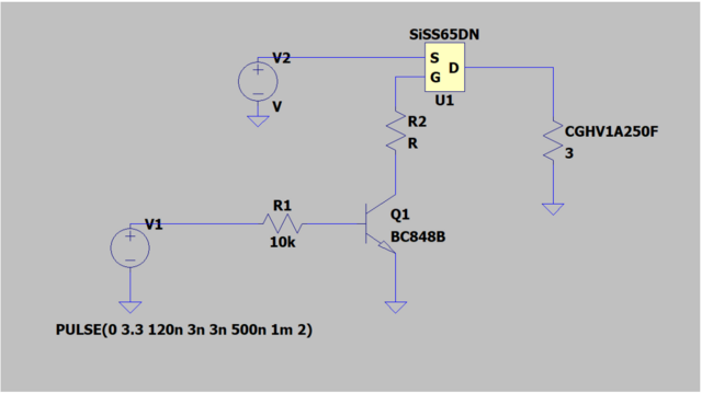
Hello ,The main goal is to Bias the CGHV1A250F transistor which is represented as 3 Ohm load resistor.shown below using PMOS shown below datasheet and spice model.LTspice file is attached with the imported spice model of the PMOS. I know the conditions for opening PMOS and NPN shown below. Suppose my pulse is in ON state. Given the diagram below,what is the strategy for formulating the current that will be flowing threw as a function of NPN and PMOS expressions? So i'll know what is the role of each element an how it influences the current going into the load resistor. Thanks. https://pdf1.alldatasheet.com/datasheet-pdf/download/1673867/WOLFSPEED/CGHV1A250F.html PMOS: https://eu.mouser.com/ProductDetail...T*MTcxNDkxNTc1My4xLjAuMTcxNDkxNTc1NS41OC4wLjA. PMOS spice model: https://www.vishay.com/doc?76129 new_model.asc
-
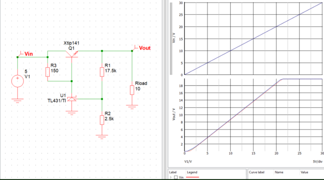
Hello ,The circuit below is a voltage regulator. It takes 24V and turns it into 20V automatickly no matter what load . It can be 10Ohm it can be 5Ohms the voltage on the load stays the same. I want to make this circuit regulate by a switch pulse.so i need to put a mosfet or BJT some where. Is there a clever analog logic you could reccomend that i will make the voltage regulation turn on and off by a switch,so i could try and simulate it? Thanks.
-
Update:Maybe the solutio is as shown below' I need some how to make 24V into 20V and make it pulsating open and close like the V2 because currently forsing steady 20V which is not good. is athere something that could be done?or any better solution? Thanks.

-
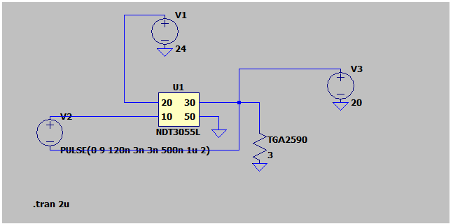
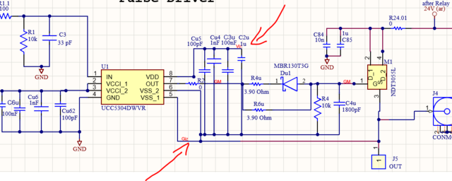
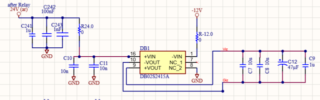
Hello,The output of DB02S2415A difference is 15V , this floating voltage supply goes into UCC5304DWVR which creates again a floating voltage for NDT3055L NMOS. This floating voltage opens the NMOS and current goes threw from drain to source. The problem starts with the parts that is not present in the schematics. I need to connect TGA2590 power amplifier to J4 node. It needs 20V on the drain. How do i make sure i have the desired 20V on that node and get the current of the NDT3055L(which was opened by the floating voltage of UCC5304DWVR)? If there is some method i could use? because this floating voltage is confusing. i am used to this of voltage where each node has exact voltage with respect to some reference. Thanks.
-
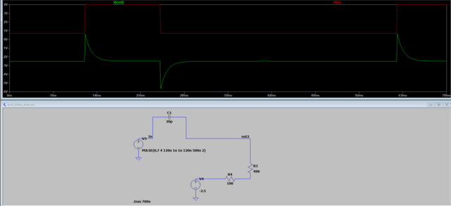
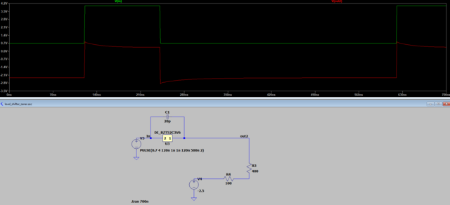
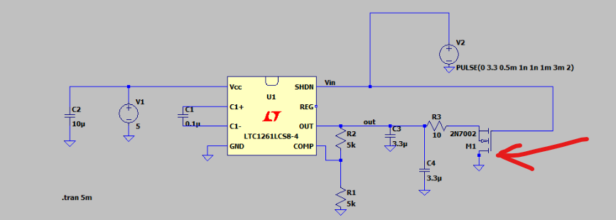
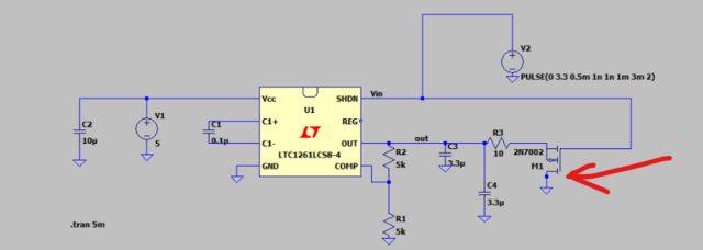
Hello MegaVolt, Sorry for not being clear enough ,currently the is a pulse of 0 till 3.3 going into the mosfet as shown below in the red arrow. I want to take this signal and to do some thing so i will get a signal shifted by some -X volts. Plain gave an intresting solution which i woul try to incorporate but they need an extra power supply ,Is there some zenner diode trick as i shown in the first post? Without adding extra power supply? Thanks.
-
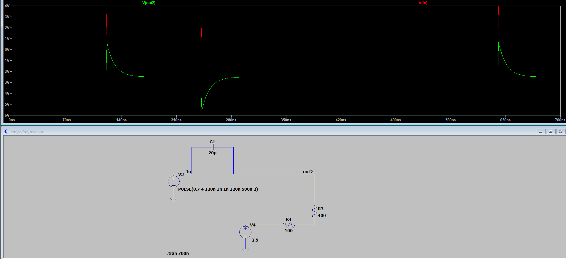
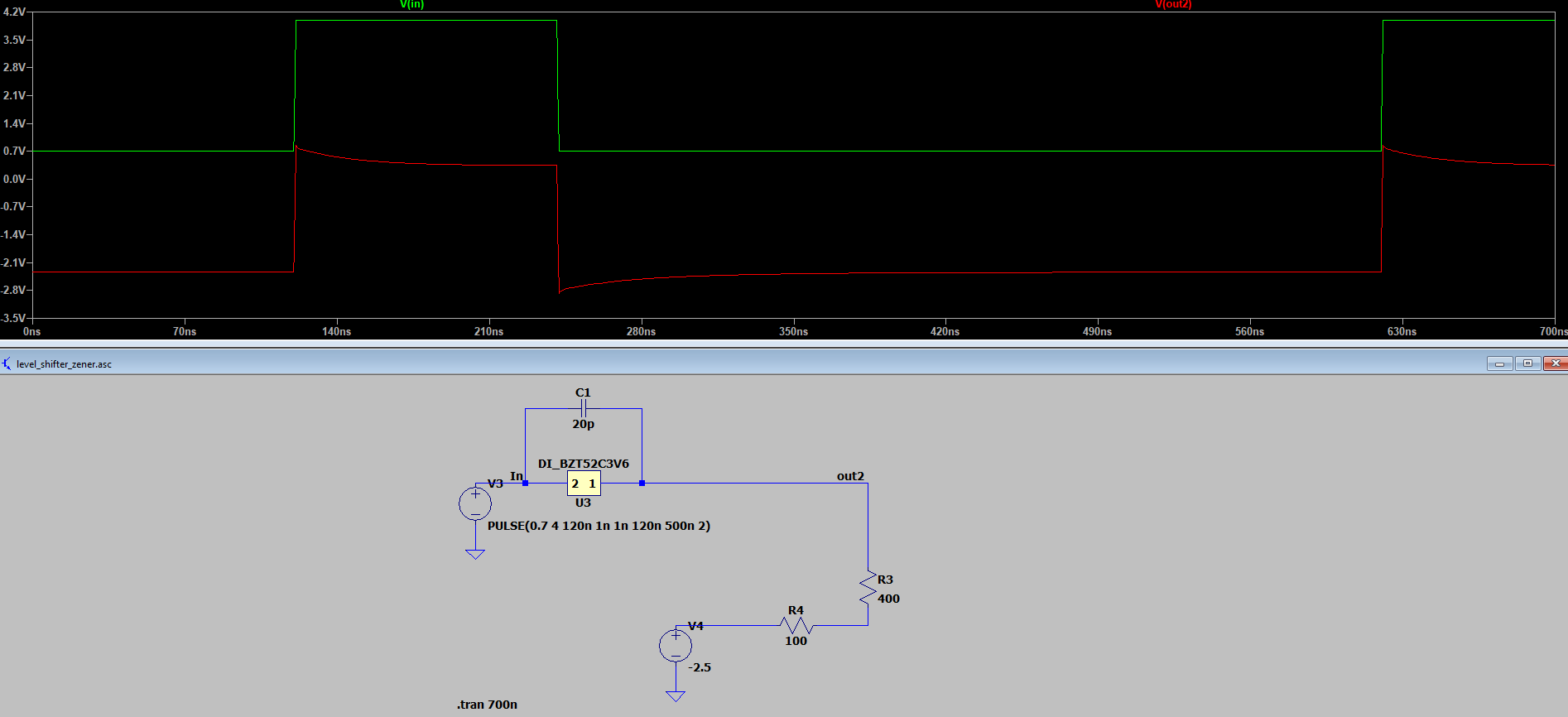
Level shifting intuition for DC-DC switching.
sergey23 опубликовал тема в Вопросы аналоговой техники
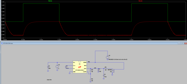
Hello,I am fluent Russian reader and speaker , however I have lots of mistakes when I write, so if its comfortable with the members of this forum I can perfectly understand your answers. I have saw a circuit shown below which is R-C integrator with a Zener diode and the ZENER diode performs a level shift with the amount of its reversed bias voltage. In the End there is a photo of a DC-DC simulation photo I have built.SHDN discharges signal at 3.3V(GPIO '1') and attached with LTC1261LCS8-4.asc I want to do the same trick here ,to send a pulse of 0 till 3.3 and using some Zener diode to get -3.6 till -0.3 for example. Is there a way to implement the same zener diode level shifting or other clever way to shift the pulse ? Thanks. level_shifter_zener.asc LTC1261LCS8-4.asc